Week 8: Electronics Production
This week focuses on understanding and documenting the in-house PCB production process as a group, and individually designing, fabricating, and testing a custom microcontroller development board.
Group Assignment
This report presents our group's collaborative experience in characterizing the process of fabricating printed circuit boards (PCBs) in our lab. We carefully documented key parameters such as feed rates, spindle speeds, depths of cut, and tooling setups, while also reflecting on the workflow from start to finish.
Characterization of Design Rules
| Parameter | Value |
|---|---|
| Feed Rate (X/Y) | 120 mm/min |
| Plunge Rate (Z) | 60 mm/min |
| Spindle Speed | 10,000 RPM |
| Cut Depth (Traces) | 0.1 mm |
| Cut Depth (Outline) | 0.8 mm |
| Tooling | V-bit (0.4 mm), End mill (1.0 mm) |
Workflow for PCB Manufacturing (Boardhouse)
- Create and verify the PCB design.
- Generate Gerber files and drill files from the design software.
- Validate the files using Gerber viewers.
- Submit files to a PCB fabrication service (boardhouse).
- Confirm order specifications and make payment.
- Receive and inspect fabricated PCBs upon delivery.
PCB Fabrication Process (In-House)
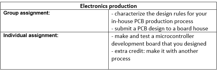
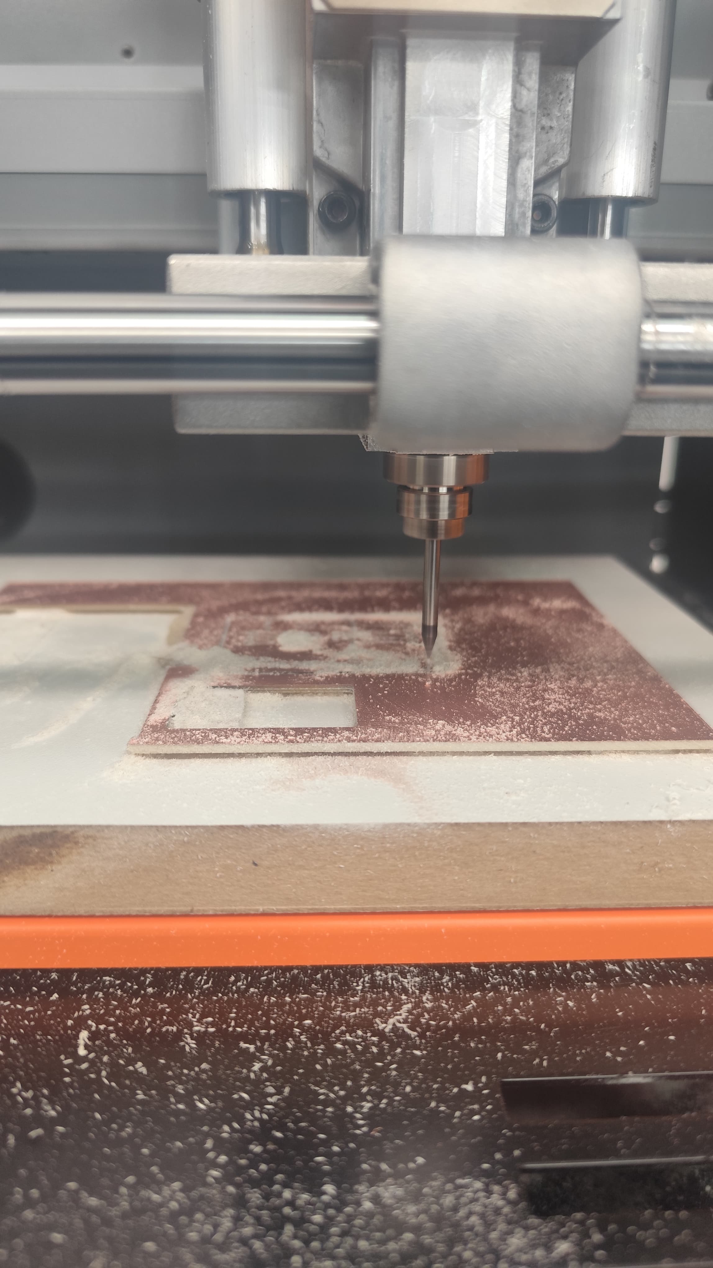
1. Equipment Used: Monofab SRM-20
Our team used the Monofab SRM-20 CNC milling machine, known for its precision on FR-4 or phenolic copper-clad boards. It proved ideal for our prototyping needs.
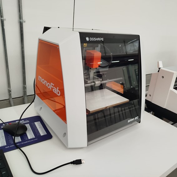
For the track width, we must calculate based on the current our circuit will handle. In this case, all the elements are designed to operate at less than 1 amp.


In the Kicad program we use a track width slightly larger than the suggested one, which is 1 mm.
2. Initial Test Run
To ensure everything was working properly, we started with a standard test design. This allowed us to verify the basic setup and machine functionality before moving on to custom designs.
3. Calibration Design Selection
We selected specific calibration patterns from the Fab Academy library. These are designed to help verify the accuracy and alignment of the machine across small and detailed geometries.
4. Preview and Design Check
As a group, we thoroughly reviewed the PCB design in our CAD software to confirm the geometry was correct and error-free before exporting.
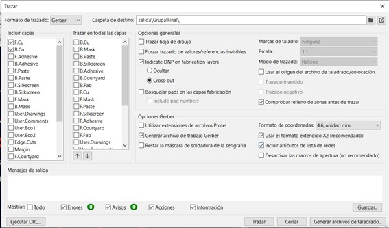
5. Generating Gerber and Drill Files
We exported the required Gerber files for traces and the accompanying drill files. This step was crucial for preparing the layout for the milling process.
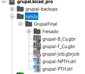
6. File Management
All generated files were saved and organized for easy import into FlatCAM during the toolpath generation stage.
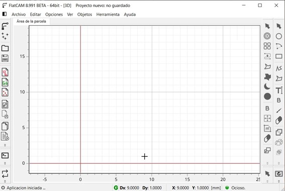
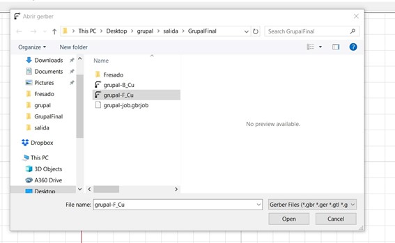
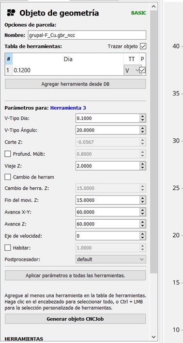
7. FlatCAM Setup
Using FlatCAM, we imported the Gerber and drill files to create toolpaths. This software allowed us to fine-tune machining parameters before generating the final G-code.
8. Reviewing in FlatCAM
We carefully examined the imported files to ensure trace alignment and correct toolpath generation.
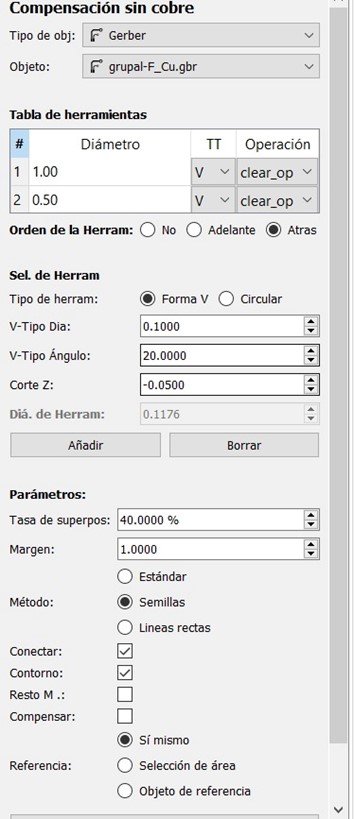
9. Tool Selection
Our team opted for V-bit tools (typically 0.4 mm) for the trace isolation milling and a 1 mm flat end mill for the board outline.
10. Machining Parameter Configuration
We configured the CNC settings as follows: 120 mm/min feed rate, 60 mm/min plunge rate, 0.1 mm depth of cut for traces, 0.8 mm for outline cuts, and spindle speeds ranging from 8000 to 12000 RPM.
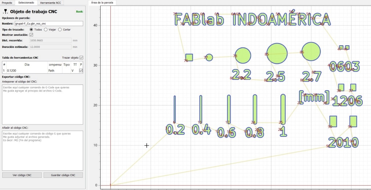
11. G-Code Generation
FlatCAM generated the final G-code files, which we saved for use in the SRM-20 milling software.
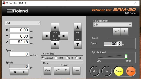
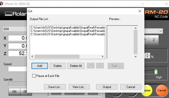
12. Machine Setup on SRM-20
We established the zero point (G54) on the material surface, ensuring alignment before starting the job.
13. Loading Files to the CNC
The previously generated G-code was loaded onto the SRM-20 interface, and we confirmed all settings matched our defined parameters.
14. Z-Axis Calibration
We carefully adjusted the tool height on the Z-axis using a manual calibration process to ensure the first layer cut through the copper surface cleanly.
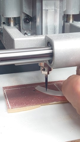
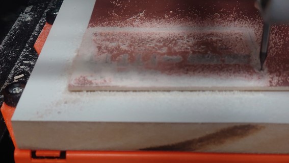
15. Milling Process
The CNC milling process was initiated. Each team member took turns supervising the job, checking for consistent toolpaths and material removal.
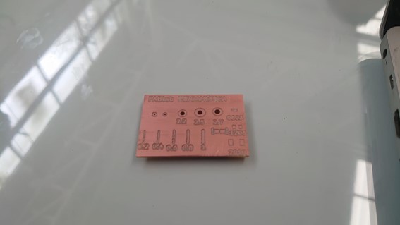
16. Final PCB Output
The result was a clean, precisely milled PCB with accurate traces and a defined board outline, ready for component soldering.
Conclusion and Group Reflection
This project allowed us to collaboratively explore each stage of the PCB fabrication process. From design to milling, we gained hands-on experience in toolpath generation, machine calibration, and file management. We also learned to work as a team, ensuring quality control at every step and troubleshooting minor issues together. The process enhanced our understanding of digital fabrication and PCB prototyping workflows.
Individual Assignment
Electronics manufacturing involves designing, fabricating, assembling, and testing electronic components and devices. For this individual assignment, I focused on creating a custom microcontroller development board based on the ATtiny412, documenting the entire process from design to testing.
1. Design Preparation
The process began with preparing the design for the microcontroller circuit board. I started by selecting the ATtiny412 microcontroller and determining the necessary components. To ensure proper connections, I conducted research and reviewed the microcontroller’s datasheet, which provided critical information about its pinout and requirements.
2. Circuit Design
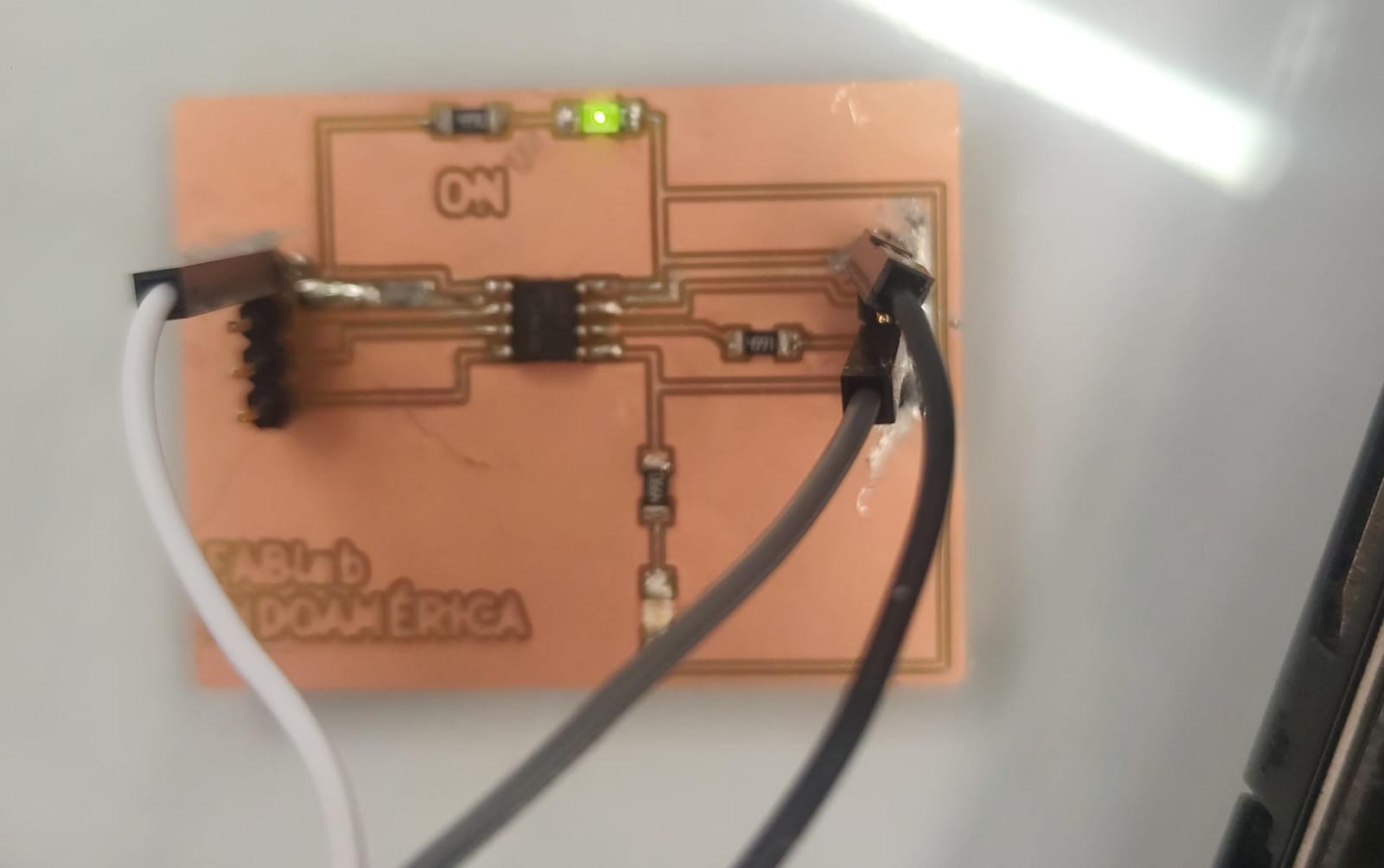
After studying the datasheet, I designed the circuit, incorporating ports for all input, output, and power pins. A 4.7 kΩ resistor was added to the UPDI port to enable program uploading. I included an LED as an output on one of the pins to verify program execution and another LED to indicate power status. The circuit is powered with a 5V supply.
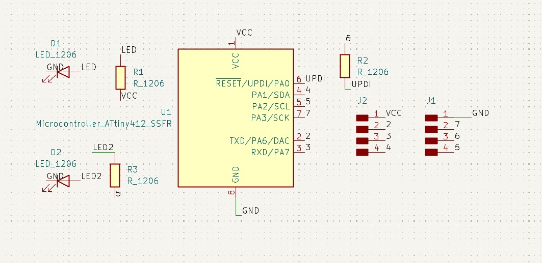
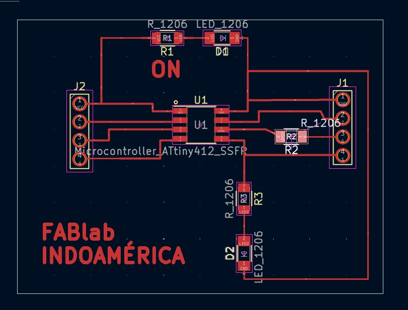
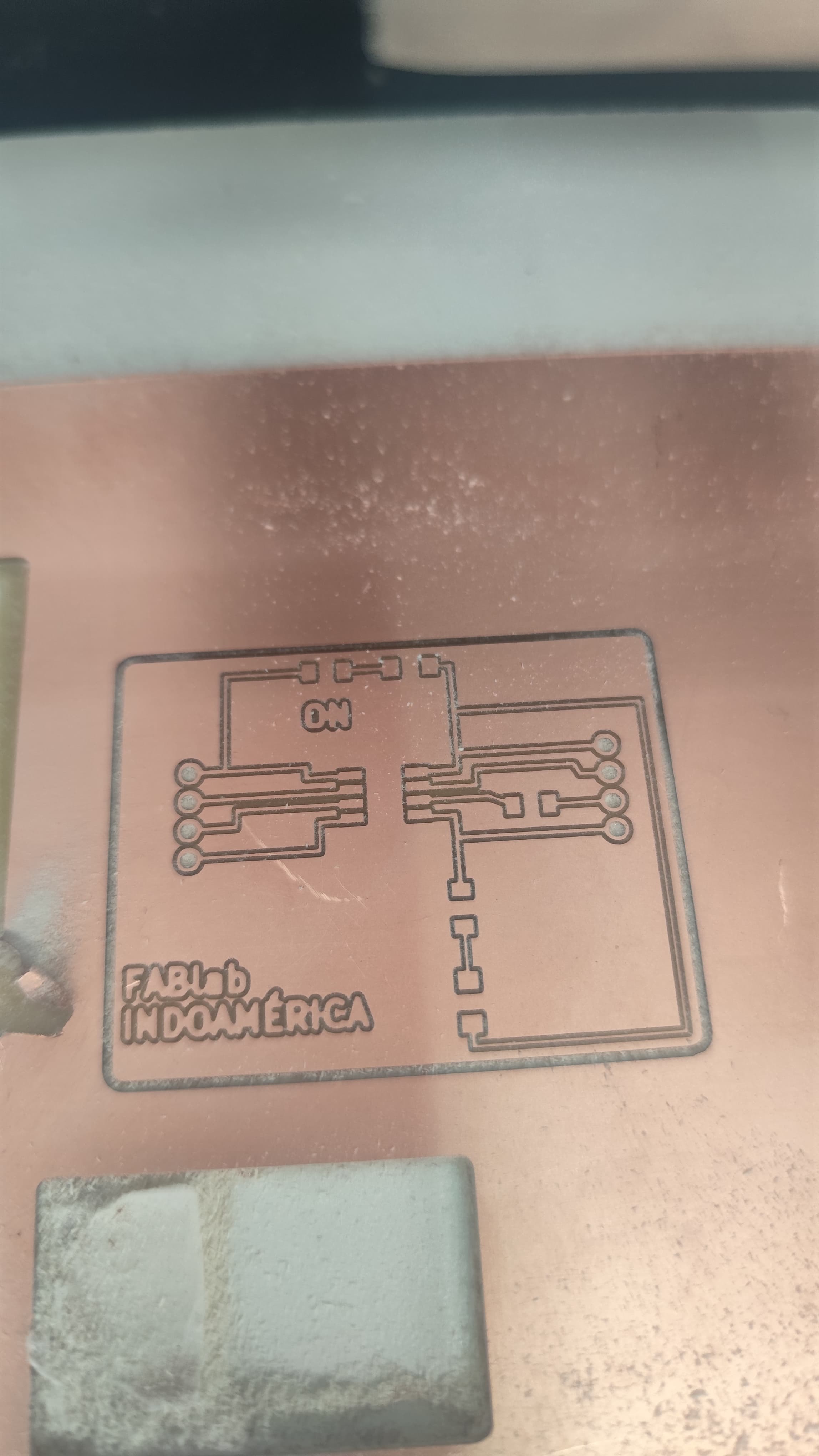
3. PCB Design with FAB Library
The PCB design was created using the FAB library from Fab Academy, which includes traces and electronic components tailored for such projects. This ensured compatibility and ease of fabrication. Once the design was finalized, I exported the Gerber and drill files for the next step.
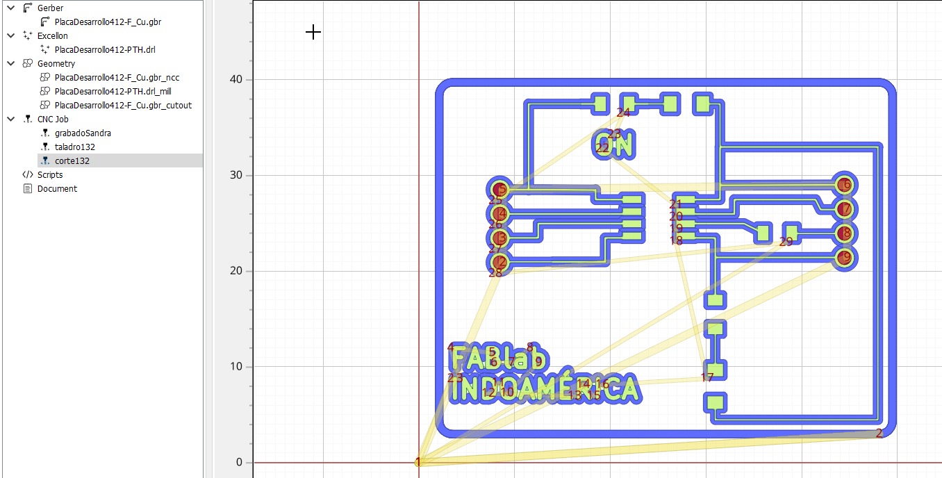
4. Toolpath Generation in FlatCAM
Using the Gerber and drill files, I opened FlatCAM to configure the machining parameters, including speeds, tools, and trajectories. This step generated the G-code files necessary for milling the PCB on the SRM-20 machine.
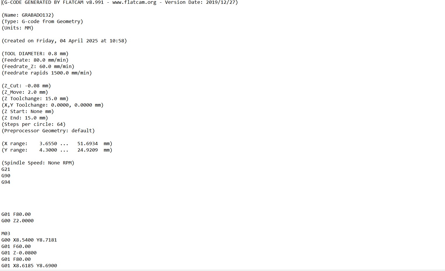
5. G-code Generation
The G-code is generated automatically by the FlatCAM program, where parameters such as speeds, tool used, tool paths, part number, and tracking distances are specified. This code guides the milling machine during the fabrication process.
6. PCB Fabrication
I loaded the G-code files into the SRM-20 software and initiated the milling process. The machine precisely cut the traces and outline of the board, resulting in a clean PCB ready for assembly.
7. Finished PCB Board
After milling, the PCB was completed with well-defined traces and outlines, ready for component soldering.
8. Soldering Components
I soldered the components onto the PCB, including the ATtiny412, resistors, LEDs, and connectors. Quality soldering was essential to ensure reliable electrical connections and proper functionality of the board.
9. Programming Setup
To program the ATtiny412, I used an Arduino Nano as a programmer. I connected it to the board via the UPDI pin and configured the Arduino IDE accordingly.
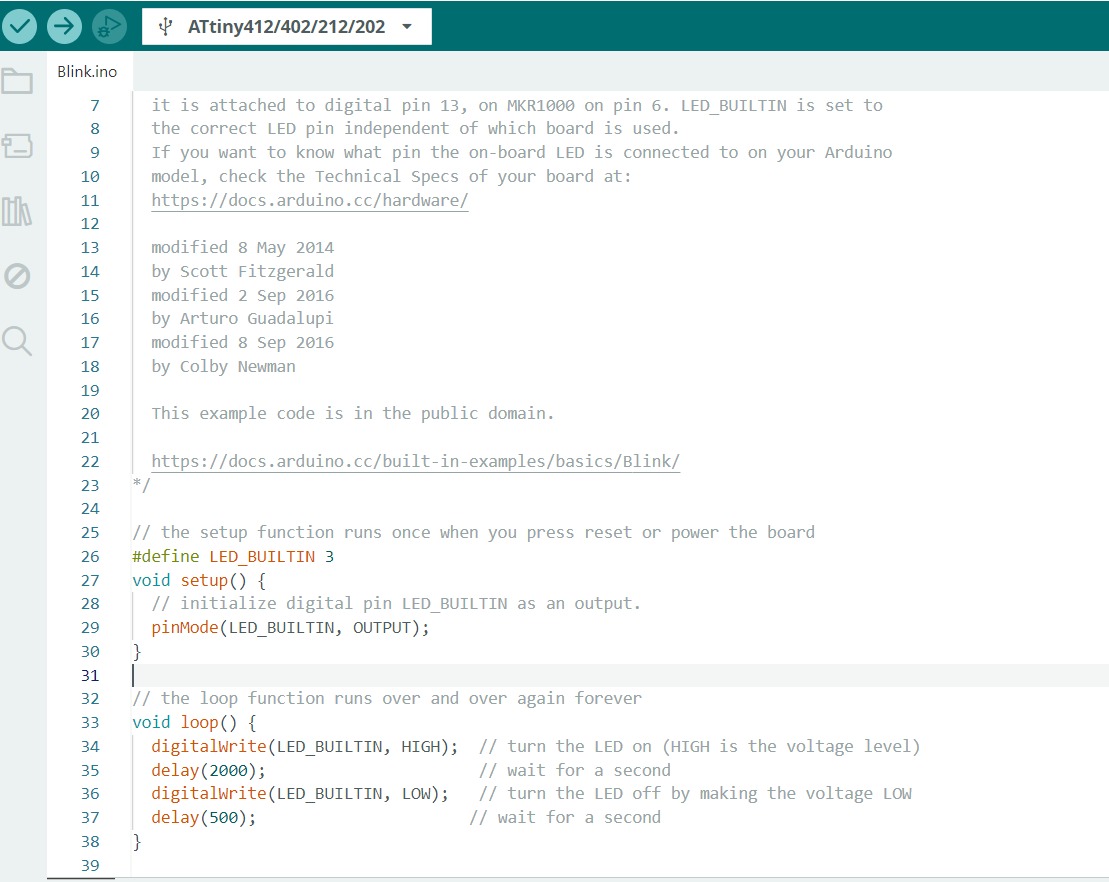
10. Testing the Board
In the Arduino IDE, I selected the ATtiny412 board and the appropriate COM port. I uploaded a test program to turn on the LED connected to pin 4, verifying the board’s operation. The successful blinking of the LED confirmed that the design, fabrication, and programming were all functioning correctly.
11. Operation of the Development Board
Below is a video demonstrating the operation of the development board in action, showing the LED responding to the uploaded program.
Week 8: Conclusion
This individual assignment was a rewarding experience that allowed me to apply the skills learned during the group assignment. Designing and fabricating my own microcontroller development board deepened my understanding of electronics production, from circuit design to PCB milling and soldering. Testing the board with a simple LED program confirmed its functionality and highlighted the importance of precision at every step. This process has equipped me with valuable hands-on knowledge for future projects in digital fabrication.